Long-Term Stability and Productivity for Advanced Process Control and Development
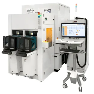
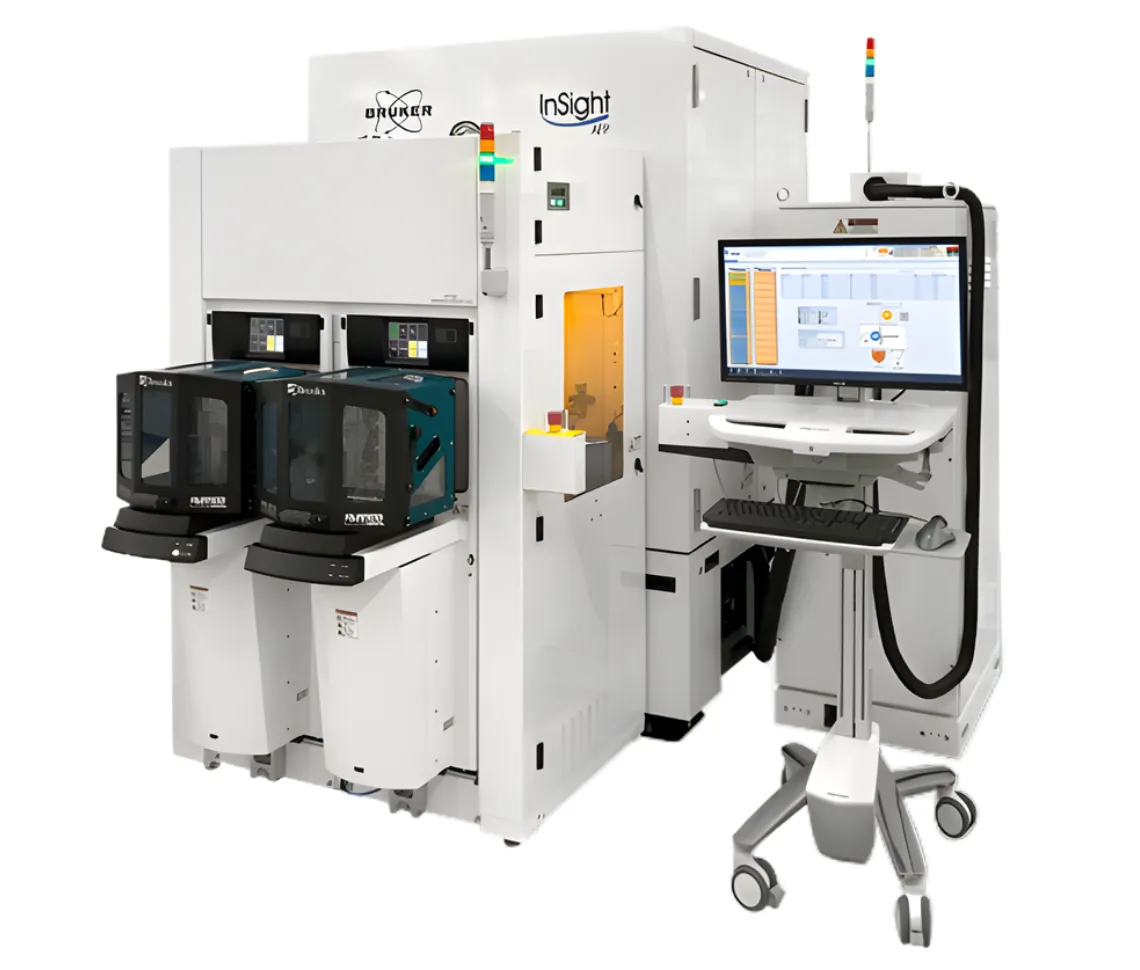
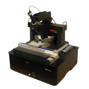
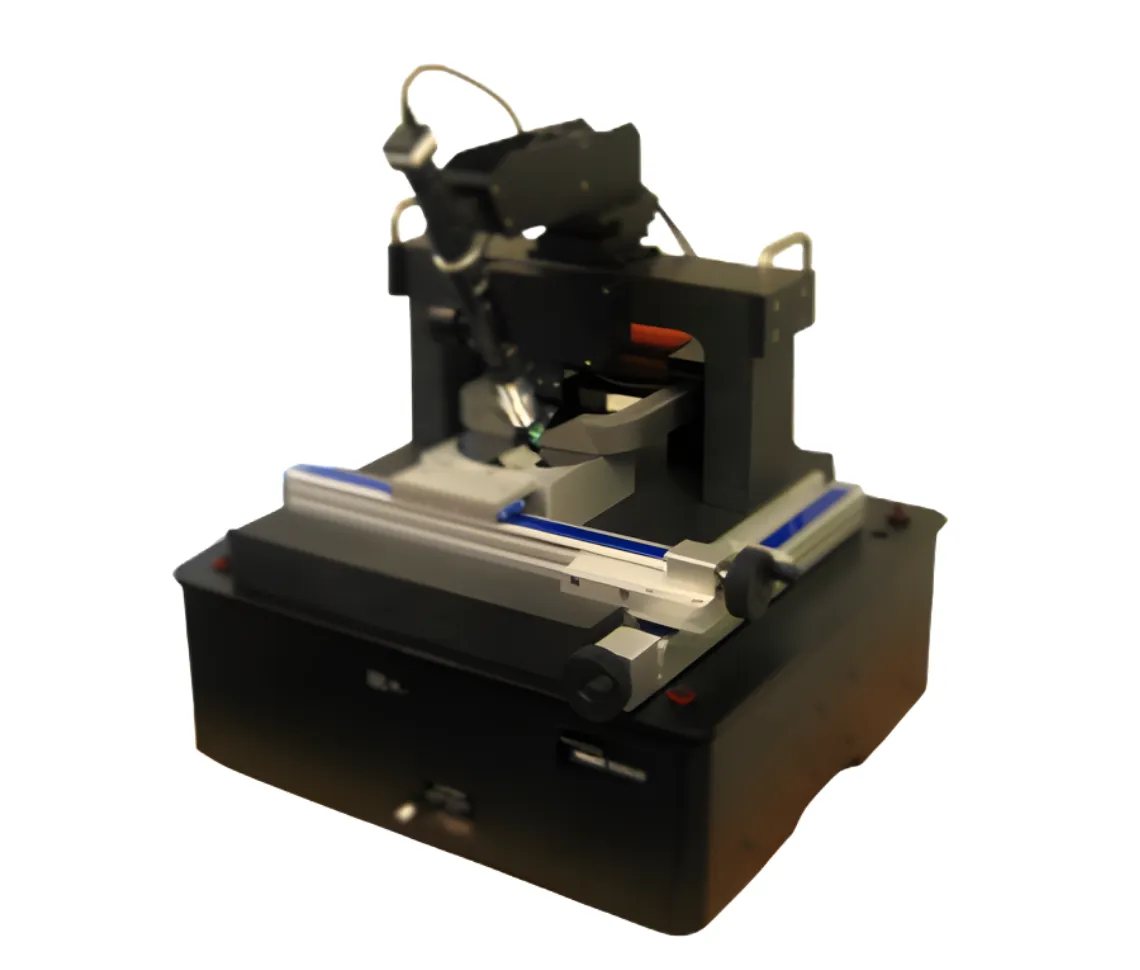
InSight AFP is the world’s highest performance and industry preferred CMP profiling and etch depth metrology system for advanced technology nodes. The combination of its modern tip scanner with inherently stable capacitive gauges and an accurate air-bearing positioning system enables non-destructive, direct measurements in the active area of dies.
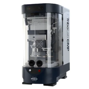
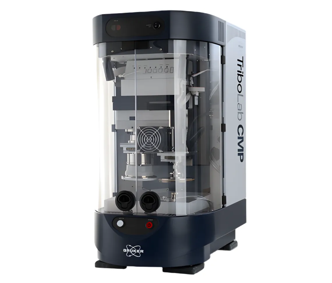
Leveraging over 20 years of CMP characterization expertise with its predecessor product (Bruker CP-4), TriboLab CMP brings a complete set of capabilities to the industry-leading TriboLab platform. The resulting accuracy and measurement repeatability enables the highly effective qualification, inspection, and ongoing functionality testing required throughout the CMP process. TriboLab CMP is the only process development tool on the market that can provide a broad range of polishing pressure (0.05-50 psi), speeds (1 to 500 rpm), friction, acoustic emissions, and surface temperature measurements for accurate and complete characterization of CMP processes and consumables.
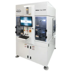
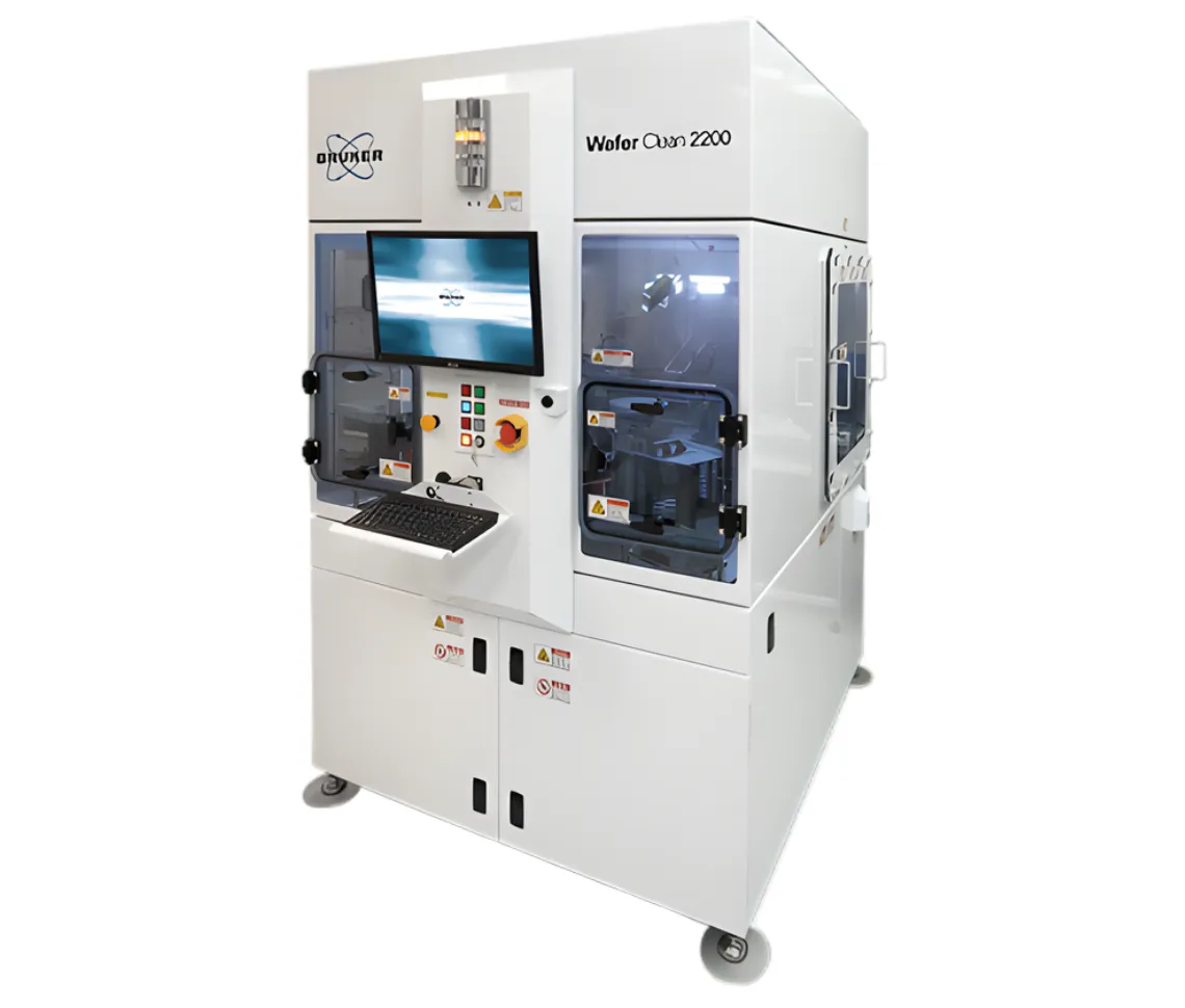
The Bruker Wafer Clean 2200 System removes particulate contamination and thin film organic residues from silicon, compound semiconductor, MEMS and thin film head substrates using a unique carbon dioxide (CO2) snow cleaning process. CO2 snow cleaning is fast, environmentally friendly and non-damaging. The all-dry process offers numerous advantages over conventional wet and plasma cleaning techniques. This fully automated, high volume production system is field proven with over 100 systems running 24/7 in high volume production applications around the globe.
The SmartProber-P1 is aimed at the next-generation over 5.5 kOe. Various configurations of this type of SmartProber are available. If the high perpendicular field is required, but only small samples need to be measured, the automated wafer stage can be replaced with a cheaper manual stage.
SP-P1 – 6kOe magnet, 300mm rotary wafer-stage
Configuration options:
C: Additional in-plane magnet module with a field strength of 2kOe
Y: 200mm XY wafer-stage
M: Manual wafer-stage for small samples
L: 10kOe magnet
This low-cost table-top equipment comes with manual x-y positioning, fully automated probe landing, an in-plane magnet as well as an anti-vibration table. The open nature, low cost, and versatility make the
SmartProber-TT especially suited for research and/or development.
Sample size: up to 6″ wafers, up to 1.3 mm thickness
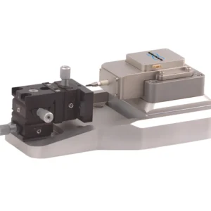
Bruker’s Hysitron BioSoft In-Situ Indenter is a first-of-its-kind instrument specifically designed for multiscale quantitative mechanical testing of biological materials and soft matter, such as hydrogels. BioSoft synchronizes powerful mechanical and optical characterization techniques to achieve a comprehensive understanding of the mechanics of biomaterials. This portable system integrates with existing inverted optical microscopes to bring advanced biomechanical testing capabilities into your laboratory.
Bruker’s Hysitron BioSoft In-Situ Indenter is a first-of-its-kind instrument specifically designed for multiscale quantitative mechanical testing of biological materials and soft matter, such as hydrogels. BioSoft synchronizes powerful mechanical and optical characterization techniques to achieve a comprehensive understanding of the mechanics of biomaterials. This portable system integrates with existing inverted optical microscopes to bring advanced biomechanical testing capabilities into your laboratory.
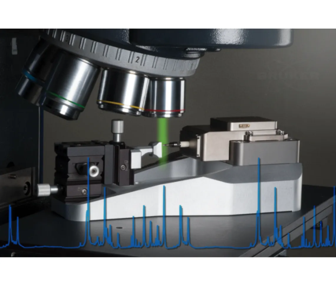
Bruker’s Hysitron IntraSpect 360 brings quantitative mechanical property characterization to X-Ray microscopes (XRM) and beamlines. This unique system can be used to perform a variety of mechanical tests such as indentation, compression, fatigue, and bending, which can then be correlated to 2D or 3D images from the host microscope.